
10 GHz 25 W GaN power amplifier
Mar 4, 2026
Good results had previously been achieved on 10 GHz EME using 10–12 W into a 1.2 m dish. Over the winter period, the decision was made to increase transmit power to approximately 25 W by constructing a higher-power amplifier stage.
With no prior experience in building RF power amplifiers at microwave frequencies, a substantial amount of time was spent reviewing published designs, conference proceedings, application notes and device data sheets. Detailed notes and test results were maintained throughout, helping to identify problems and make appropriate modifications.
CMPA801B025
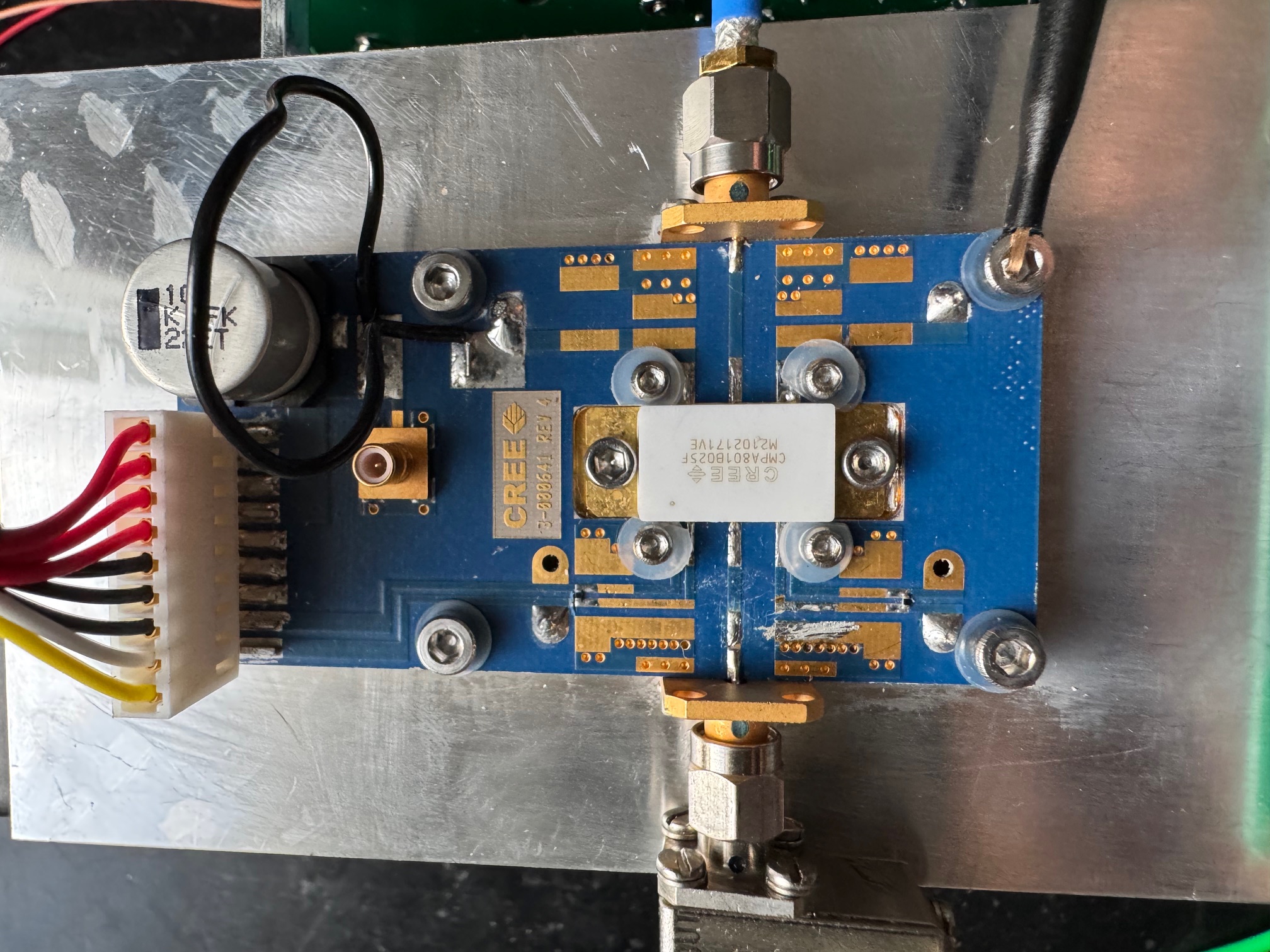
Several devices were evaluated against the required frequency coverage and output power. The device selected was the CMPA801B025, a 8.5–11.0 GHz GaN MMIC specified for 16 dB gain and 45 dBm (32 W) output power at 10 GHz. Originally produced by Cree and discontinued in 2020, these devices and evaluation boards are still available through various distribution channels. (Cree rebranded as Wolfspeed in 2021, and its RF business was subsequently acquired by MACOM in late 2023.)
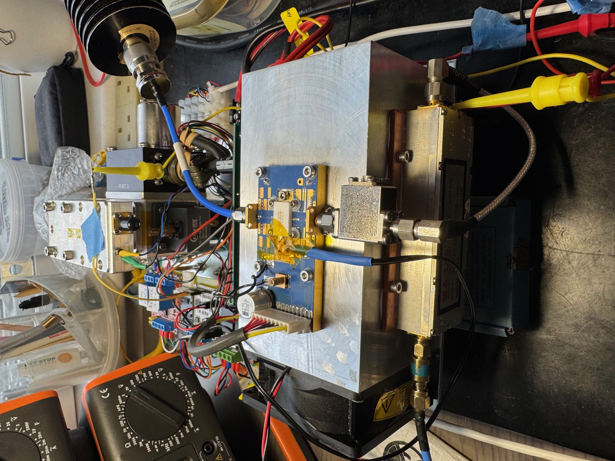
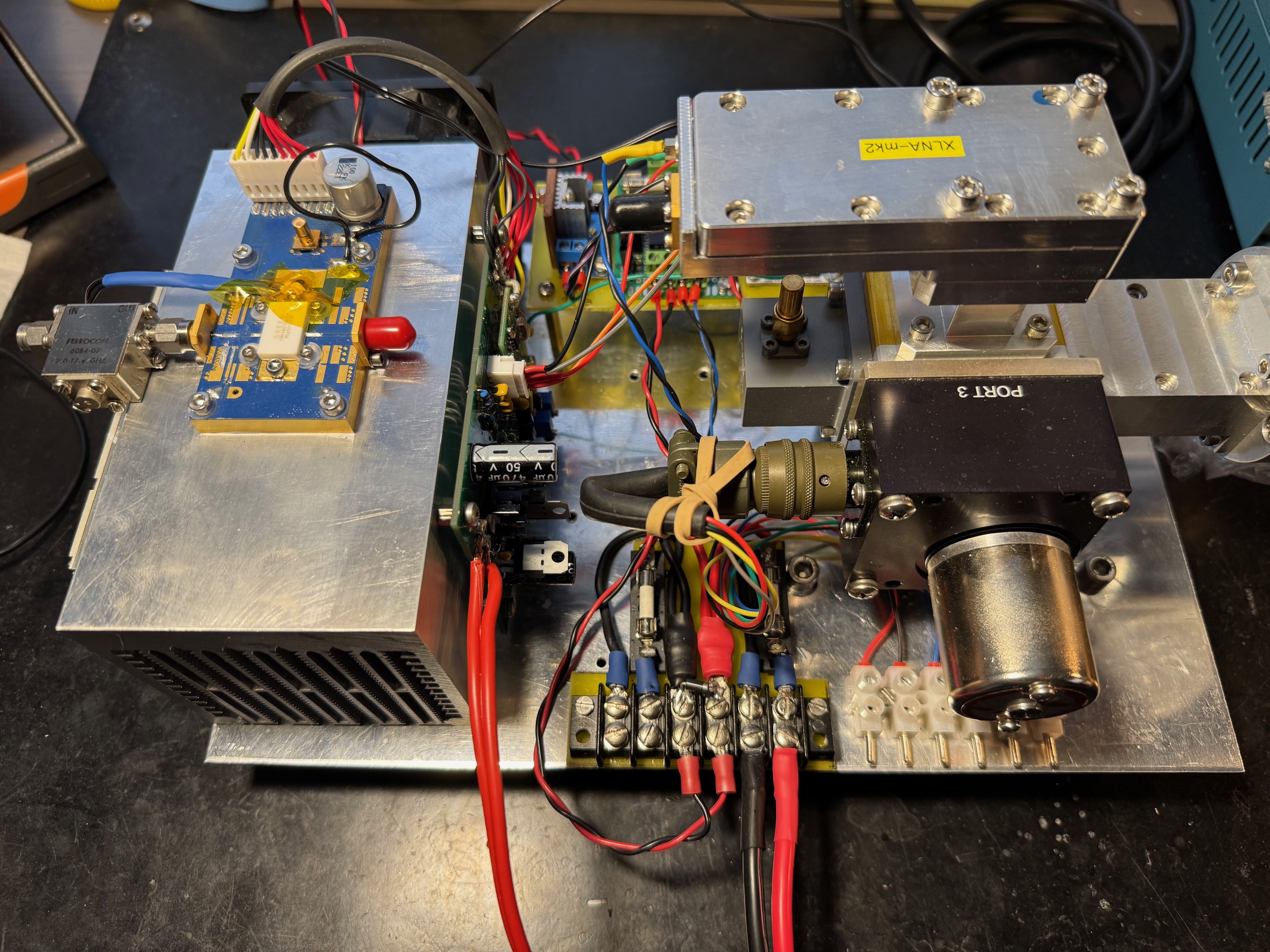
An evaluation board with the device pre-mounted on a copper spreader was obtained. This avoided the need to design a RF board or mount the device, allowing effort to focus instead on biasing, sequencing, thermal management, and system integration.
Biasing and Sequencing
A well-known rule for GaN devices is that drain voltage must never be applied without an established gate bias. Particular care was taken to design a bias and control circuit that would be robust and fail-safe when integrated into the existing 10 GHz station hardware.
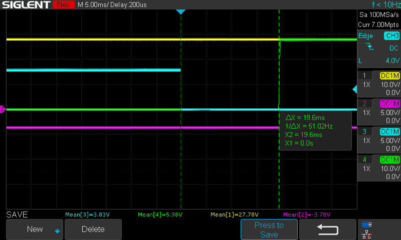
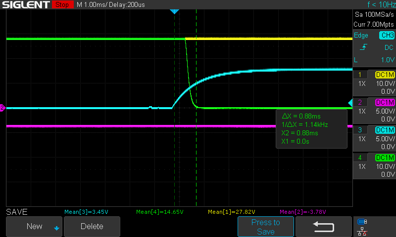
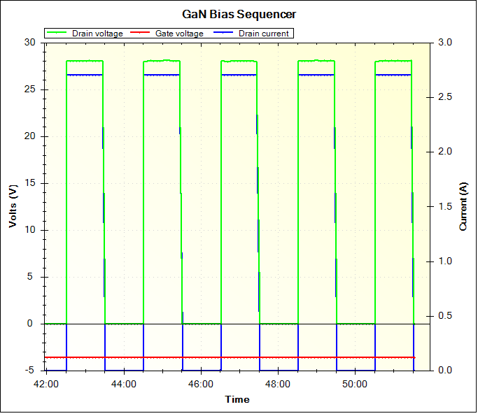
The amplifier is powered from a 28 V SMPS. Gate bias is present whenever the bias board is energised, and MOSFET interlocking prevents the drain supply from being enabled unless valid gate bias is detected. Drain bias is controlled by the existing Arduino-based sequencer, on during transmit and off during receive. The sequencer also manages the waveguide switch and transmit inhibit, ensuring RF drive is confined to the drain-on interval [1], [2], [3].
Voltage, current, and temperature are monitored via MODBUS sensors already used elsewhere in the station.
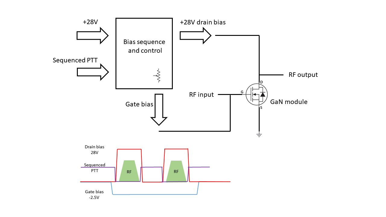
After simulating several bias arrangements, a modified version of the K5TRA/PA0HRK/ON4BCB design was adopted [4], [5]. The principal modification was adapting the drain switching logic to operate from an existing PTT line that is pulled low during transmit. A breadboard prototype was constructed and tested into a DC load with an oscilloscope to confirm the interlock and sequencing before designing a PCB.
Thermal Management
At the intended operating point, 25 W RF output power would require an estimated 105 W DC input power. This corresponds to a device dissipation of roughly 80 W under full-drive conditions.
Based on this dissipation level, thermal calculations indicated that a heatsink with a thermal resistance of approximately 0.2 °C/W would provide sufficient margin for operation at ambient temperatures up to 50 °C.
A Fischer LA9/150 heatsink profile was selected, as it met the required thermal specification and adequate surface area to mount the PA evaluation board, driver amplifier, and bias circuitry together. This arrangement simplified integration and minimised interconnecting lead lengths.
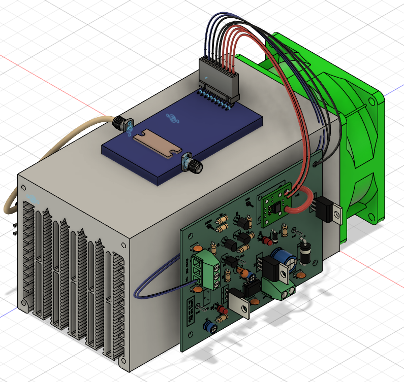
Initial Tests
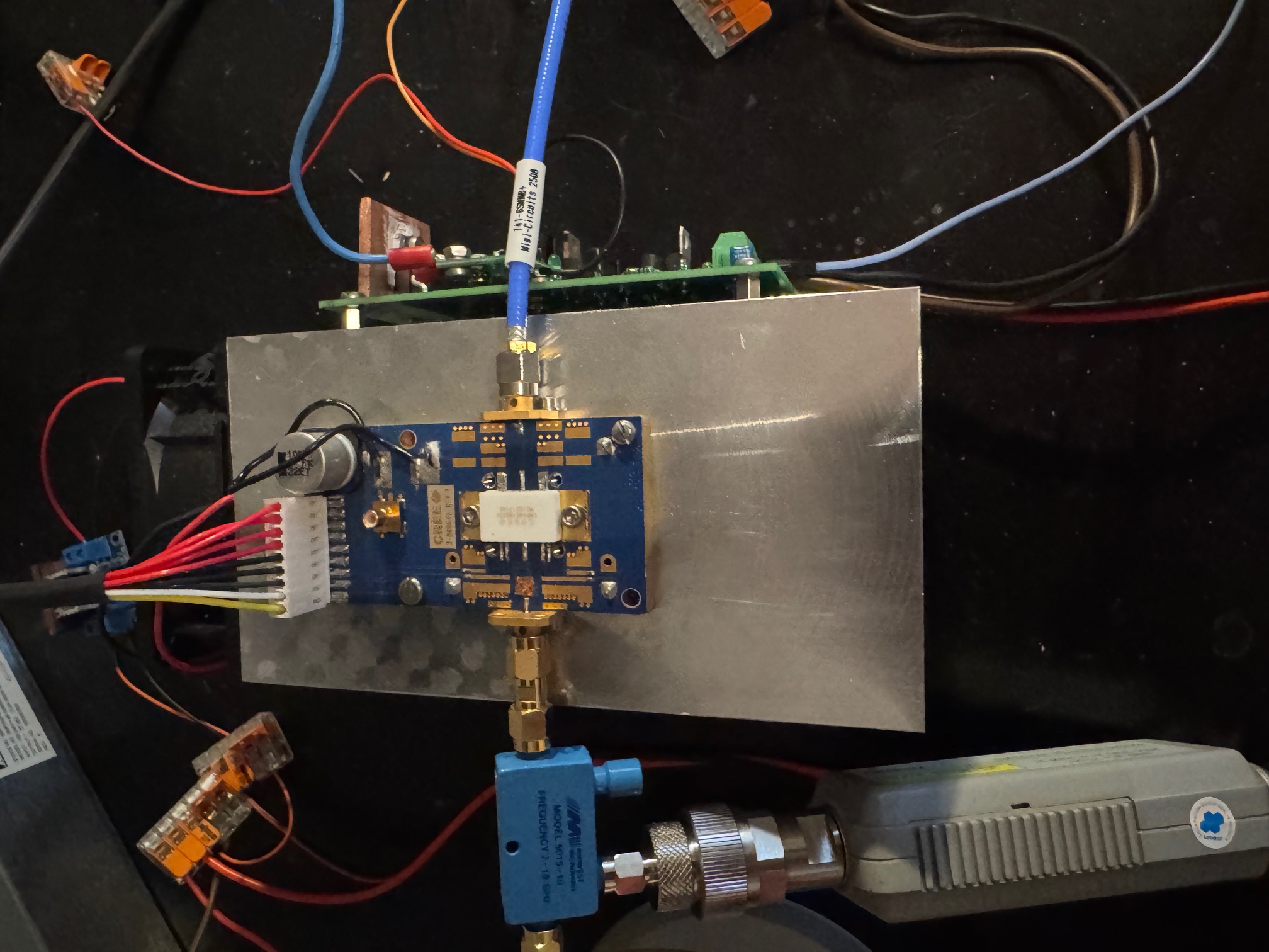
The assembled bias board passed initial DC and timing checks without issue. A Cree checklist and similar guidance provided by Charlie, DL3WDG [6], were followed to test the RF board and set the quiescent drain current (Idq).
With the RF board mounted on a heatsink and terminated in 50 Ω at both ports, the bias board was connected to a variable bench supply set to 15 V. The gate voltage (Vgg) was verified at −4.6 V (beyond cutoff) before applying drain voltage (Vdd). The supply voltage was gradually increased to 28 V and there was zero drain current.
Gate bias was then adjusted to set Idq to 1.2 A; however, this required Vgg ≈ −2.98 V rather than the expected −2.7 V. Although not fully appreciated at the time, this represented the first indication that operating conditions differed to the datasheet.
Small-signal measurements at 28 V with input levels between −20 dBm and 0 dBm showed approximately 20 dB gain — around 4 dB below the specified value. Drain current remained stable at 1.2 A. At this stage, to improve recording of operating conditions during testing, an ACS724 current sensor and Arduino UNO were added to log Idd and Vdd in real time using MegunoLink [7][8]. This setup proved invaluable for analysing behaviour during drive sweeps.
Large-signal testing with a driver amplifier revealed that saturation occurred at 25–26 dBm input, roughly 4 dB earlier than anticipated. Measured output power was approximately 41 dBm. Input matching was briefly investigated by modifying the microstrip (“snowflaking”), but little improvement was obtained, consistent with the device’s internal matching.
At this stage, thermal limitation was suspected. Although the copper spreader was secured at the four corners, the threaded holes adjacent to the device had not been used. After drilling and tapping corresponding holes in the aluminium heatsink, additional fasteners were installed. Nylon washers were placed under the screws near the microstrip lines to minimise the risk of shorting them out. (Thanks to John, G4BAO for making these suggestions).
Despite these changes, gain remained several dB below expectation.
Independent Gate Bias Controllers
Attention then turned to the internal two-stage structure of the MMIC. The evaluation board allows independent control of the gate bias for each stage, Vgg1 and Vgg2, and the board was modified accordingly. A second bias network was added on a small piece of stripboard so that each stage could be adjusted independently. With Vgg1 set to −2.7 V and Vgg2 to −2.6 V, Idq was 1.2 A. Large-signal gain had improved slightly (≈1 dB), suggesting progress.
However, while rearranging wiring in preparation for final installation, abrupt jumps in drain current were observed when Vgg1 approached −3 V and Vgg2 still near cutoff. With no suitable spectrum analyser available, a diode detector connected to the output confirmed that the amplifier was oscillating without RF drive. The absence of gate damping resistors was identified as the likely cause. Earlier tests had used relatively long bias leads, unintentionally stabilising the circuit. Once the wiring was shortened, the instability became evident.
Adding 20 Ω series resistors in each gate bias line eliminated the oscillation. With both gates set to −2.7 V, Idq stabilised at 1.2 A and remained well-behaved.
Final Testing
With the damping resistors in place, small-signal measurements were repeated. Gain at −20 dBm and 0 dBm input now closely approached datasheet values.
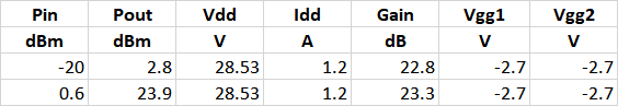
Large-signal sweeps from 20 dBm to 33 dBm input showed performance close to specification, with no observable instability. Saturated output and gain compression behaviour were consistent with the device data sheet.
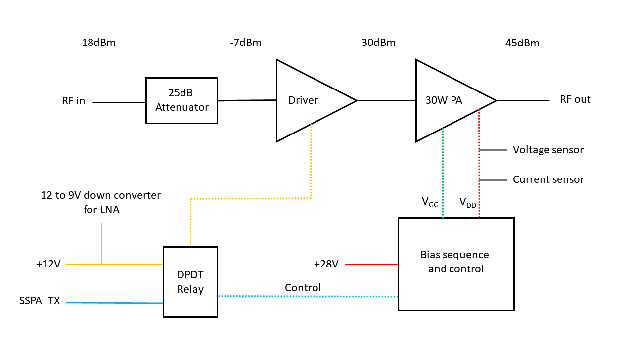
System Integration
The completed 10 GHz system consists of an IC-705 and Arduino sequencer in the shack, an SMPS/transverter assembly mounted on the dish feedarm, and the driver amplifier, SSPA, and LNA mounted on the feedtray.
MODBUS sensors monitor voltage, current, and temperature at the dish. Data are polled by an Arduino and displayed locally, with over-temperature and over-current thresholds implemented for protection.
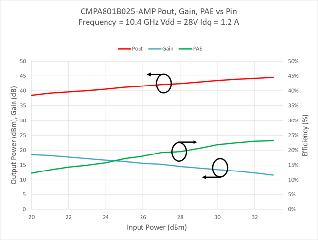
Final bench testing was conducted with all modules mounted on the feedtray and all cabling in place. A thermistor mounted on the device flange was used to monitor temperature. Drive levels from the IC-705 and transverter were adjusted to account for cable losses, resulting in approximately 30 dBm input to the GaN RF board. Soak testing, using WSJT-X Q65 60D 1 minute on, 1 minute off periods showed an increase in temperature of around 20 °C, with good recovery during the receive cycle.
Conclusion
This project has been a steep learning curve and at 10 GHz, bias sequencing, mechanical detail and stability measures are as critical as the RF design itself.
For a novice builder, the manufacturer’s evaluation board for the RF section simplified the project. Performance shortfalls were ultimately traced to two factors: incomplete mechanical mounting near the device and gate-stage oscillation masked by wiring parasitics. Independent gate control provided valuable diagnostics and the 20 Ω series gate resistors restored stable operation.
References
- [1] How to Bias GaN Transistors: An Introduction Tutorial, Qorvo Inc., 2015
- [2] A Versatile bias supply for Depletion Mode GaAs & GaN Power Amplifiers
- [3] Portable 3 cm EME with a 1 meter Offset Fed Dish, Al Ward, W5LUA - slide 9 and 10
- [4] 12 W 10 GHz Station, Tom Apel, K5TRA - slide 44
- [5] EME SSPA’s voor 23 en 3 cm, Harke Smits, PA0HRK
- [6] Charlie Suckling, G3WDG, A 50W GaN Solid State Power Amplifier for 10GHz, DUBUS, 1/2015, pp 27 - 37
- [7] Pololu ACS724 Current Sensor Carriers
- [8] MegunoLink